|
|
Crystallographic Texture |
|
|
Electron Backscattering Patterns and Ion Blocking Patterns Automated Crystal Orientation Microscopy (ACOM), or in short Orientation Microscopy (OM), on bulk surfaces is usually based on Backscatter Kikuchi Diffraction (BKD) in the SEM. A commercial acronym for this technique is EBSD. Spatial resolution is usually in the range of 0.05 μm, accuracy is better than 0.5°, and speed of on-line measurement is actually more than 1000 patterns per second with Fast EBSD. An alternative technique yielding higher spatial resolution is microbeam electron diffraction in the TEM or SEM using spot (SAD) or transmission Kikuchi patterns (TKD). Thin foils, however, are difficult to prepare for observation in transmission and, even worse, are sources of orientation errors due to wrinkling which is frequently manifested by bend contours. The study of fine grain and heavily deformed materials in general, of nanomaterials, of recrystallization, grain growth and the characterization of grain boundaries demand for a substantially higher spatial resolution than is achieved with EBSD in the SEM.
Diffraction
patterns can be produced not only by electrons, but as well by ions of
some ten keV kinetic energy when impinging on a crystalline surface.
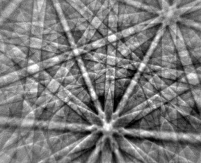
The first Ion Blocking Patterns (IBP) have been published by A.F.
Tulinov in 1965 [1, 2]. The patterns
have been produced by proton beams of 150, 200, and 500 keV steered onto
a single crystal of W respectively Mo at an angle of incidence of 30°.
They have been recorded on special photographic plates, placed parallel
with the surface of the crystal, to cover a large solid angle. Patterns have been indexed in these papers and in
further papers published in the same year by A.F. Tulinov and
co-workers, so providing evidence of the crystallographic nature of the
patterns and of the mechanism of their generation by channeling the
ions along low-index lattice planes and crystallographic directions.
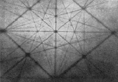
IBP
have, at a first glimpse, an appearance substantially different from
Backscatter Kikuchi Patterns (BKP):
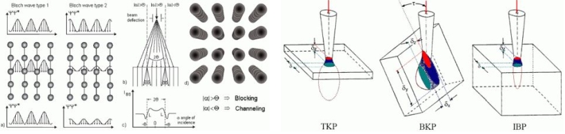
Kikuchi patterns are clearly generated by diffraction, whereas IBP could perhaps be better interpreted by the classical ballistic model of channeling. Precise experimental measurements are still missing so as to decide whether Bragg's equation is valid here. The background is produced by blocked ions according to Rutherford scattering. There is no significant difference in backscattering from an amorphous and from a crystalline solid for ions that impinge at directions off the critical angles (~ Bragg angles). At kinetic energies in the range of several ten keV, their mean free paths are less than a few atomic layers. Only the channeled ions are missing in case of a crystal, they penetrate deep in the crystal and form sharp cusps of low intensity on the background. So the background intensity can be used as signal. This information about the crystal structure comes from the upmost atomic layers, like Auger electrons. As a consequence, spatial resolution in IBP is only limited by the diameter of the primary beam probe. On the other hand, BKP are formed by electrons that are backscattered from the interaction volume that extends beneath the surface to a depth of the mean free path of energetic electrons. Hence spatial resolution in EBSD is limited to some ten nanometer, despite that the electron beam can easily be focused to a significantly smaller probe size. The geometrical basics of IBP and BKP, however, are quite similar. The center line of a band corresponds to the section line of the - imaginarily extended - diffracting lattice plane with the recording plane. The crossing points of bands, named poles, represent the positions of zone axes of the crystal. So the crystal structure and crystal orientation of the diffracting volume can be determined from the intensity distribution and positions of the bands in an IBP in quite a similar way as in a BKP. As an application, C.S. Barrett and co-workers [3] have used proton blocking patterns at 100 keV for phase differentiation. Crystallographic aspects of ion beam scattering have been discussed in a review article [4]. A commercial instrument for the identification and rapid alignment of single crystals was manufactured by Edwards High Vacuum Intern. [5]. ________ [2] A.F: Tulinov, V.S.
Kulikauskas and M.M. Malov: Proton scattering from a tungsten single
crystal. Physics Letters 18 (1965) 304-307 The
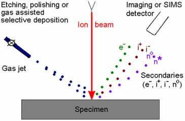
working principles of ion scanning microscopes and of the more common
Scanning Electron Microscopes (SEM) are very similar, with the
exception of an ion gun and electrostatic or quadrupol lenses which
replace the electron gun and round magnetic lenses. Ion scanning
microscopes are used in the microelectronic industry to repair masks
and electronic circuits. Focused Ion Beam (FIB) appliances to the SEM
or stand-alone ion scanning microscopes with a Liquid Metal Ion Source
(LMIS) ( Ga+ ) are frequently employed in materials science for the
preparation of TEM and SEM specimens by ion milling. Bulk surfaces are
imaged in scanning mode whereby ion induced electrons, backscattered
primary ions, secondary ions which have been released from the sample,
neutrals or cathodoluminescense radiation are used as signals.
A
similar technique as for BKD has been proposed for the acquisition and
indexing of Ion Blocking Patterns (IBP) in an ion scanning microscope
[2]. Orientation microscopy with IBP promises the following advantages
over EBSD in the SEM: However, beam current in small ion probes is presently very low in the Orion® Ion Scanning Microscope, so that we did not yet succeed in producing sequences of IBP. A more feasible alternative may be a stand-alone FIB ion microscope with a Ga+ LMIS, but to the disadvantage of less spatial resolution.
________ |

|